- 您现在的位置:买卖IC网 > Sheet目录328 > IDT709279L9PFG (IDT, Integrated Device Technology Inc)IC SRAM 512KBIT 9NS 100TQFP
IDT709279/69S/L
High-Speed 32/16K x 16 Synchronous Dual-Port Static RAM
Preliminary
Industrial and Commercial Temperature Ranges
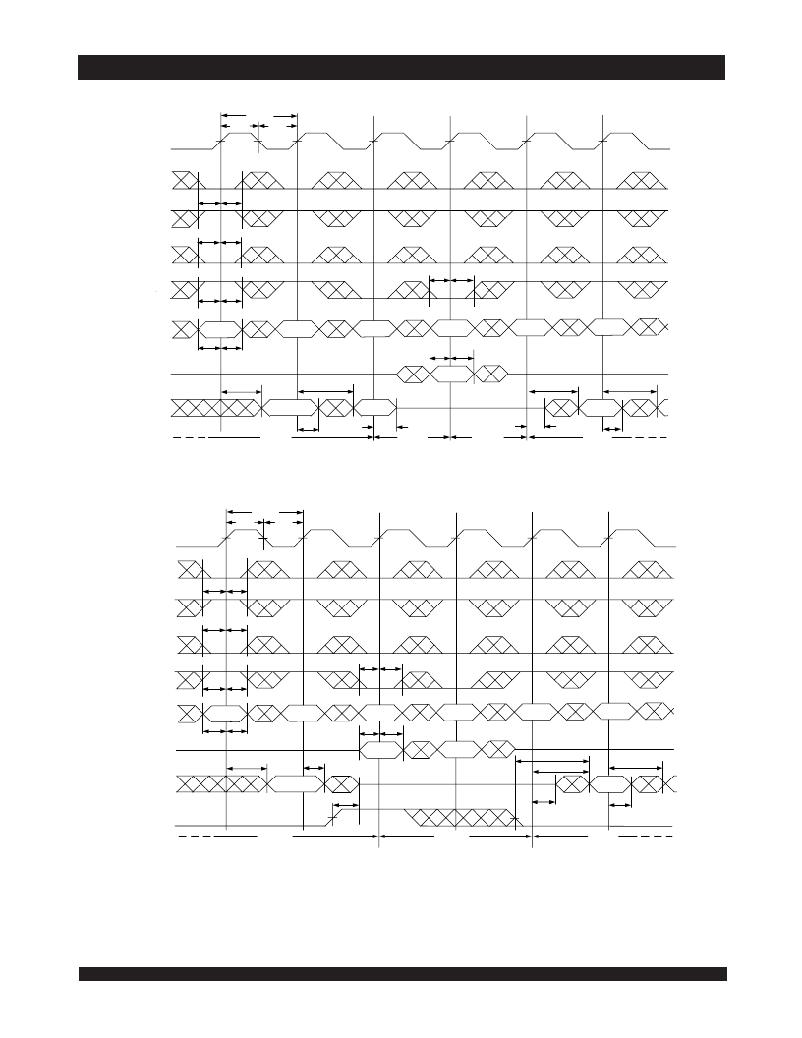
Timing Waveform of Flow-Through Read-to-Write-to-Read ( OE = V IL ) (3)
t CYC1
CLK
CE 0
t CH1
t CL1
CE 1
t SC
t SB
t HC
t HB
UB , LB
t SW t HW
R/ W
t SW t HW
(4)
ADDRESS
An
An +1
An + 2
An + 2
An + 3
An + 4
t SA
t HA
t SD t HD
DATA IN
Dn + 2
DATA OUT
(2)
t CD1
Qn
t CD1
Qn + 1
t CD1
Qn + 3
t CD1
t CKLZ
t DC
t CKHZ
(1)
(1)
t DC
READ
NOP
(5)
WRITE
READ
3243 drw 13
Timing Waveform of Flow-Through Read-to-Write-to-Read ( OE Controlled) (3)
t CYC1
CLK
CE 0
CE 1
t CH1
t SC t HC
t CL1
t SB
t HB
UB , LB
t SW t HW
R/ W
t SW t HW
(4)
ADDRESS
An
An +1
An + 2
An + 3
An + 4
An + 5
t SA
t HA
t SD t HD
DATA IN
(2)
t CD1
t DC
Dn + 2
Dn + 3
t OE
t CD1
t CD1
DATA OUT
Qn
(1)
Qn + 4
t OHZ
(1)
t CKLZ
t DC
OE
READ
WRITE
READ
3243 drw 14
NOTES:
1. Transition is measured 0mV from Low or High-impedance voltage with the Output Test Load (Figure 2).
2. Output state (High, Low, or High-impedance is determined by the previous cycle control signals.
3. CE 0 , UB , LB , and ADS = V IL ; CE 1 , CNTEN , and CNTRST = V IH .
4. Addresses do not have to be accessed sequentially since ADS = V IL constantly loads the address on the rising edge of the CLK; numbers are for reference use
only.
5. "NOP" is "No Operation." Data in memory at the selected address may be corrupted and should be re-written to guarantee data integrity.
13
6.42
发布紧急采购,3分钟左右您将得到回复。
相关PDF资料
IDT709289L9PFI
IC SRAM 1MBIT 9NS 100TQFP
IDT709359L7BFI
IC SRAM 144KBIT 7NS 100FBGA
IDT709379L7PFG
IC SRAM 576KBIT 7NS 100TQFP
IDT70P257L55BYGI
IC SRAM 128KBIT 55NS 100BGA
IDT70P258L55BYI
IC SRAM 128KBIT 55NS 100BGA
IDT70T3339S200BCG
IC SRAM 9MBIT 200MHZ 256BGA
IDT70T3509MS133BP
IC SRAM 36MBIT 133MHZ 256BGA
IDT70T3519S133DRI
IC SRAM 9MBIT 133MHZ 208QFP
相关代理商/技术参数
IDT709279S12
制造商:GEFANUC 功能描述:
IDT709279S12PF
功能描述:IC SRAM 512KBIT 12NS 100TQFP RoHS:否 类别:集成电路 (IC) >> 存储器 系列:- 标准包装:1,000 系列:- 格式 - 存储器:RAM 存储器类型:SRAM - 双端口,同步 存储容量:1.125M(32K x 36) 速度:5ns 接口:并联 电源电压:3.15 V ~ 3.45 V 工作温度:-40°C ~ 85°C 封装/外壳:256-LBGA 供应商设备封装:256-CABGA(17x17) 包装:带卷 (TR) 其它名称:70V3579S5BCI8
IDT709279S12PF8
功能描述:IC SRAM 512KBIT 12NS 100TQFP RoHS:否 类别:集成电路 (IC) >> 存储器 系列:- 标准包装:45 系列:- 格式 - 存储器:RAM 存储器类型:SRAM - 双端口,异步 存储容量:128K(8K x 16) 速度:15ns 接口:并联 电源电压:3 V ~ 3.6 V 工作温度:0°C ~ 70°C 封装/外壳:100-LQFP 供应商设备封装:100-TQFP(14x14) 包装:托盘 其它名称:70V25S15PF
IDT709279S15PF
功能描述:IC SRAM 512KBIT 15NS 100TQFP RoHS:否 类别:集成电路 (IC) >> 存储器 系列:- 标准包装:1,000 系列:- 格式 - 存储器:RAM 存储器类型:SRAM - 双端口,同步 存储容量:1.125M(32K x 36) 速度:5ns 接口:并联 电源电压:3.15 V ~ 3.45 V 工作温度:-40°C ~ 85°C 封装/外壳:256-LBGA 供应商设备封装:256-CABGA(17x17) 包装:带卷 (TR) 其它名称:70V3579S5BCI8
IDT709279S15PF8
功能描述:IC SRAM 512KBIT 15NS 100TQFP RoHS:否 类别:集成电路 (IC) >> 存储器 系列:- 标准包装:45 系列:- 格式 - 存储器:RAM 存储器类型:SRAM - 双端口,异步 存储容量:128K(8K x 16) 速度:15ns 接口:并联 电源电压:3 V ~ 3.6 V 工作温度:0°C ~ 70°C 封装/外壳:100-LQFP 供应商设备封装:100-TQFP(14x14) 包装:托盘 其它名称:70V25S15PF
IDT709279S9PF
功能描述:IC SRAM 512KBIT 9NS 100TQFP RoHS:否 类别:集成电路 (IC) >> 存储器 系列:- 标准包装:1,000 系列:- 格式 - 存储器:RAM 存储器类型:SRAM - 双端口,同步 存储容量:1.125M(32K x 36) 速度:5ns 接口:并联 电源电压:3.15 V ~ 3.45 V 工作温度:-40°C ~ 85°C 封装/外壳:256-LBGA 供应商设备封装:256-CABGA(17x17) 包装:带卷 (TR) 其它名称:70V3579S5BCI8
IDT709279S9PF8
功能描述:IC SRAM 512KBIT 9NS 100TQFP RoHS:否 类别:集成电路 (IC) >> 存储器 系列:- 标准包装:1,000 系列:- 格式 - 存储器:RAM 存储器类型:SRAM - 双端口,同步 存储容量:1.125M(32K x 36) 速度:5ns 接口:并联 电源电压:3.15 V ~ 3.45 V 工作温度:-40°C ~ 85°C 封装/外壳:256-LBGA 供应商设备封装:256-CABGA(17x17) 包装:带卷 (TR) 其它名称:70V3579S5BCI8
IDT709289L12PF
功能描述:IC SRAM 1MBIT 12NS 100TQFP RoHS:否 类别:集成电路 (IC) >> 存储器 系列:- 标准包装:1,000 系列:- 格式 - 存储器:RAM 存储器类型:SRAM - 双端口,同步 存储容量:1.125M(32K x 36) 速度:5ns 接口:并联 电源电压:3.15 V ~ 3.45 V 工作温度:-40°C ~ 85°C 封装/外壳:256-LBGA 供应商设备封装:256-CABGA(17x17) 包装:带卷 (TR) 其它名称:70V3579S5BCI8
